
TI – TPIC6595
The TPIC6595 is a monolithic, high-voltage, high-current power 8-bit shift register designed for use in systems that require relatively high load power. The device contains a built-in voltage clamp on the outputs for inductive transient protection. Power driver applications include relays, solenoids, and other medium-current or high-voltage loads.
This device contains an 8-bit serial-in, parallel-out shift register that feeds an 8-bit D-type storage register. Data transfers through both the shift and storage registers on the rising edge of the shift-register clock (SRCK) and the register clock (RCK) respectively. The storage register transfers data to the output buffer when shift-register clear (SRCLR)\ is high. When SRCLR\ is low, the input shift register is cleared. When output enable (G)\ is held high, all data in the output buffers is held low and all drain outputs are off. When G\ is held low, data from the storage register is transparent to the output buffers. The serial output (SER OUT) allows for cascading of the data from the shift register to additional devices.
Outputs are low-side, open-drain DMOS transistors with output ratings of 45 V and 250-mA continuous sink current capability. When data in the output buffers is low, the DMOS-transistor outputs are off. When data is high, the DMOS-transistor outputs have sink current capability.
Separate power and logic level ground pins are provided to facilitate maximum system flexibility. Pins 1, 10, 11, and 20 are internally connected, and each pin must be externally connected to the power system ground in order to minimize parasitic inductance. A single-point connection between pin 19, logic ground (LGND), and pins 1, 10, 11, and 20, power grounds (PGND), must be externally made in a manner that reduces crosstalk between the logic and load circuits.
The TPIC6595 is characterized for operation over the operating case temperature range of -40°C to 125°C.
DOWNLOADS:
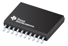
TI – TPIC6B595TI SOIC20
The TPIC6B595 device is a monolithic, high-voltage, medium-current power 8-bit shift register designed for use in systems that require relatively high load power. The device contains a built-in voltage clamp on the outputs for inductive transient protection. Power driver applications include relays, solenoids, and other medium current or high-voltage loads.
This device contains an 8-bit serial-in, parallel-out shift register that feeds an 8-bit D-type storage register. Data transfers through the shift and storage registers on the rising edge of the shift-register clock (SRCK) and the register clock (RCK), respectively.
The storage register transfers data to the output buffer when shift-register clear (SRCLR) is high. When SRCLR is low, the input shift register is cleared. When output enable (G) is held high, all data in the output buffers is held low and all drain outputs are off. When G is held low, data from the storage register is transparent to the output buffers. When data in the output buffers is low, the DMOS-transistor outputs are off. When data is high, the DMOS transistor outputs have sink-current capability. The serial output (SER OUT) allows for cascading of the data from the shift register to additional devices.
Outputs are low-side, open-drain DMOS transistors with output ratings of 50 V and 150-mA continuous sink-current capability. Each output provides a 500-mA typical current limit at TC = 25°C. The current limit decreases as the junction temperature increases for additional device protection.
The TPIC6B595 is characterized for operation over the operating case temperature range of −40°C to 125°C.
DOWNLOAD:
TLO74ST SOIC
The TL074, TL074A, and TL074B are high-speed JFET input single operational amplifiers. Each of these JFET input operational amplifiers incorporates well matched, high-voltage JFET and bipolar transistors in a monolithic integrated circuit.
The devices feature high slew rates, low input bias and offset currents, and low offset voltage temperature coefficient.
TLO84ST SOIC
The TL084I, TL084AI, TL084BI, TL084C, TL084AC and TL084BC are high-speed, JFET input, quad operational amplifiers incorporating well matched, high voltage JFET and bipolar transistors in a monolithic integrated circuit.
The devices feature high slew rates, low input bias and offset currents, and low offset voltage temperature coefficient.
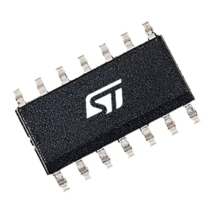
UC3843ST SOIC14
The UC284xB family of control ICs provides the necessary features to implement off-line or DC to DC fixed frequency current mode control schemes with a minimal external parts count. Internally implemented circuits include a trimmed oscillator for precise DUTY CYCLE CONTROL under voltage lockout featuring start-up current less than 0.5mA, a precision reference trimmed for accuracy at the error amp input, logic to insure latched operation, a PWM comparator which also provides current limit control, and a totem pole output stage designed to source or sink high peak current. The output stage, suitable for driving N-Channel MOSFETs, is low in the off-state.
Differences between members of this family are the under-voltage lockout thresholds and maximum duty cycle ranges. The UC2842B and UC2844B have UVLO thresholds of 16V (on) and 10V (off), ideally suited off-line applications The corresponding thresholds for the UC2843B and UC2845B are 8.5V and 7.9V. The UC2842B and UC2843B can operate to duty cycles approaching 100%. A range of the zero to < 50 % is obtained by the UC2844B and UC2845B by the addition of an internal toggle flip flop which blanks the output off every other clock cycle.