74HC00D
Quad 2-input NAND gate
Features and benefits- Total power dissipation: ≤ 590 mW
- Wide working voltage range: nominal 2.4 V to 75 V (E24 range)
- Small plastic package s
- Wide supply voltage range from 2.0 to 6.0 V
- CMOS low power dissipation
- High noise immunity
- Latch-up performance exceeds 100 mA per JESD 78 Class II Level B
- Input levels:
- For 74HC00: CMOS level
- For 74HCT00: TTL level
- Complies with JEDEC standards:
- JESD8C (2.7 V to 3.6 V)
- JESD7A (2.0 V to 6.0 V)
- ESD protection:
- HBM JESD22-A114F exceeds 2000 V
- MM JESD22-A115-A exceeds 200 V
- Multiple package options
- Specified from -40 °C to +85 °C and from -40 °C to +125 °C
- uitable for surface-mounted design
- Low differential resistance
- AEC-Q101 qualified
74HC02D
Quad 2-input NOR gate
Features and benefits- Wide supply voltage range from 2.0 V to 6.0 V
- CMOS low power dissipation
- High noise immunity
- Latch-up performance exceeds 100 mA per JESD 78 Class II Level B
- Input levels:
- For 74HC02: CMOS level
- For 74HCT02: TTL level
- Complies with JEDEC standards:
- JESD8C (2.7 V to 3.6 V)
- JESD7A (2.0 V to 6.0 V)
- ESD protection:
- HBM JESD22-A114F exceeds 2000 V
- MM JESD22-A115-A exceeds 200 V
- Multiple package options
- Specified from -40 °C to +85 °C and from -40 °C to +125 °C
74HC04D
Hex inverter
Features and benefits- Wide supply voltage range from 2.0 V to 6.0 V
- CMOS low power dissipation
- High noise immunity
- Latch-up performance exceeds 100 mA per JESD 78 Class II Level B
- Complies with JEDEC standards:
- JESD8C (2.7 V to 3.6 V)
- JESD7A (2.0 V to 6.0 V)
- Input levels:
- For 74HC04: CMOS level
- For 74HCT04: TTL level
- ESD protection:
- HBM JESD22-A114F exceeds 2000 V
- MM JESD22-A115-A exceeds 200 V
- Multiple package options
- Specified from -40 °C to +85 °C and from -40 °C to +125 °C
74HC08D
Quad 2-input AND gate
Features and benefits- Wide supply voltage range from 2.0 V to 6.0 V
- CMOS low power dissipation
- High noise immunity
- Latch-up performance exceeds 100 mA per JESD 78 Class II Level B
- Input levels:
- For 74HC08: CMOS level
- For 74HCT08: TTL level
- Complies with JEDEC standards:
- JESD8C (2.7 V to 3.6 V)
- JESD7A (2.0 V to 6.0 V)
- ESD protection:
- HBM JESD22-A114F exceeds 2000 V
- MM JESD22-A115-A exceeds 200 V
- Multiple package options
- Specified from -40 °C to +85 °C and from -40 °C to +125 °C
74HC125D
Quad buffer/line driver; 3-state
Features and benefits- Wide supply voltage range from 2.0 to 6.0 V
- CMOS low power dissipation
- High noise immunity
- Latch-up performance exceeds 100 mA per JESD 78 Class II Level B
- Complies with JEDEC standards:
- JESD8C (2.7 V to 3.6 V)
- JESD7A (2.0 V to 6.0 V)
- Input levels:
- The 74HC125: CMOS levels
- The 74HCT125: TTL levels
- ESD protection:
- HBM JESD22-A114F exceeds 2000 V
- MM JESD22-A115-A exceeds 200 V
- Specified from -40 °C to +85 °C and from -40 °C to +125 °C
74HC126D
Quad buffer/line driver; 3-state
Features and benefits- Wide supply voltage range from 2.0 to 6.0 V
- CMOS low power dissipation
- High noise immunity
- Latch-up performance exceeds 100 mA per JESD 78 Class II Level B
- Inverting outputs
- Complies with JEDEC standards:
- JESD8C (2.7 V to 3.6 V)
- JESD7A (2.0 V to 6.0 V)
- Input levels:
- For 74HC126: CMOS levels
- For 74HCT126: TTL levels
- ESD protection:
- HBM JESD22-A114F exceeds 2000 V
- MM JESD22-A115-A exceeds 200 V
- Specified from -40 °C to +85 °C and from -40 °C to +125 °C
74HC132D
Quad 2-input NAND Schmitt trigger
Features and benefits- Wide supply voltage range from 2.0 to 6.0 V
- CMOS low power dissipation
- High noise immunity
- Unlimited input rise and fall times
- Latch-up performance exceeds 100 mA per JESD 78 Class II Level B
- Complies with JEDEC standards:
- JESD8C (2.7 V to 3.6 V)
- JESD7A (2.0 V to 6.0 V)
- ESD protection:
- HBM JESD22-A114F exceeds 2000 V
- MM JESD22-A115-A exceeds 200 V
- Multiple package options
- Specified from −40 °C to +85 °C and from −40 °C to +125 °C
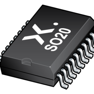
74HC132ST SOIC
The M74HC132 is a high-speed CMOS quad 2-input Schmitt NAND gate fabricated with silicon gate C2MOS technology. Pin configuration and function are identical to those of the M74HC00. The hysteresis characteristics (around 20 % VCC) of all inputs allow slowly changing input signals to be transformed into sharply defined jitter-free output signals.
All inputs are equipped with protection circuits against static discharge and transient excess voltage.
Download Datasheet:
74HC138D
3-to-8 line decoder/demultiplexer; inverting
Features and benefits- Wide supply voltage range from 2.0 to 6.0 V
- CMOS low power dissipation
- High noise immunity
- Latch-up performance exceeds 100 mA per JESD 78 Class II Level B
- Demultiplexing capability
- Multiple input enable for easy expansion
- Ideal for memory chip select decoding
- Active LOW mutually exclusive outputs
- Input levels:
- For 74HC138: CMOS level
- For 74HCT138: TTL level
- Complies with JEDEC standards:
- JESD8C (2.7 V to 3.6 V)
- JESD7A (2.0 V to 6.0 V)
- ESD protection:
- HBM JESD22-A114F exceeds 2000 V
- MM JESD22-A115-A exceeds 200 V
- Multiple package options
- Specified from -40 °C to +85 °C and from -40 °C to +125 °C
74HC14D
Hex inverting Schmitt trigger
Features and benefits- Wide supply voltage range from 2.0 to 6.0 V
- CMOS low power dissipation
- High noise immunity
- Unlimited input rise and fall times
- Latch-up performance exceeds 100 mA per JESD 78 Class II Level B
- Complies with JEDEC standards:
- JESD8C (2.7 V to 3.6 V)
- JESD7A (2.0 V to 6.0 V)
- ESD protection:
- HBM JESD22-A114F exceeds 2000 V
- MM JESD22-A115-A exceeds 200 V
- Multiple package options
- Specified from -40 °C to +85 °C and from -40 °C to +125 °C
74HC151D
8-input multiplexer
Features and benefits- Specified in compliance with JEDEC standard no. 7A
- Input levels:
- For 74HC151: CMOS level
- For 74HCT151: TTL level
- Low-power dissipation
- Non-inverting data path
- ESD protection:
-
- HBM JESD22-A114F exceeds 2000 V
- MM JESD22-A115-A exceeds 200 V
- Specified from -40 °C to +85 °C and from -40 °C to +125 °C
74HC164D
8-bit serial-in, parallel-out shift register
Features and benefits- Wide supply voltage range from 2.0 to 6.0 V
- CMOS low power dissipation
- High noise immunity
- Input levels:
- For 74HC164: CMOS level
- For 74HCT164: TTL level
- Gated serial data inputs
- Asynchronous master reset
- Complies with JEDEC standards
- JESD8C (2.7 V to 3.6 V)
- JESD7A (2.0 V to 6.0 V)
- Latch-up performance exceeds 100 mA per JESD 78 Class II Level B
- ESD protection:
- HBM JESD22-A114F exceeds 2000 V
- MM JESD22-A115-A exceeds 200 V
- Multiple package options
- Specified from -40 °C to +85 °C and -40 °C to +125 °C.
74HC165D
8-bit parallel-in/serial out shift register
Features and benefits- Wide supply voltage range from 2.0 to 6.0 V
- CMOS low power dissipation
- High noise immunity
- Latch-up performance exceeds 100 mA per JESD 78 Class II Level B
- Asynchronous 8-bit parallel load
- Synchronous serial input
- Input levels:
- For 74HC165: CMOS level
- For 74HCT165: TTL level
- Complies with JEDEC standards:
- JESD8C (2.7 V to 3.6 V)
- JESD7A (2.0 V to 6.0 V)
- ESD protection:
- HBM JESD22-A114F exceeds 2000 V
- MM JESD22-A115-A exceeds 200 V
- Multiple package options
- Specified from -40 °C to +85 °C and from -40 °C to +125 °C
74HC238D
3-to-8 line decoder/demultiplexer
Features and benefits- Wide supply voltage range from 2.0 to 6.0 V
- CMOS low power dissipation
- High noise immunity
- Demultiplexing capability
- Multiple input enable for easy expansion
- Ideal for memory chip select decoding
- Active HIGH mutually exclusive outputs
- Input levels:
- For 74HC238: CMOS level
- For 74HCT238: TTL level
- Complies with JEDEC standards
- JESD8C (2.7 V to 3.6 V)
- JESD7A (2.0 V to 6.0 V)
- Latch-up performance exceeds 100 mA per JESD 78 Class II Level B
- ESD protection:
- HBM JESD22-A114F exceeds 2000 V
- MM JESD22-A115-A exceeds 200 V
- Multiple package options
- Specified from -40 °C to +85 °C and from -40 °C to +125 °C
74HC244D
Octal buffer/line driver; 3-state
Features and benefits
- Wide supply voltage range from 2.0 to 6.0 V
- CMOS low power dissipation
- High noise immunity
- Latch-up performance exceeds 100 mA per JESD 78 Class II Level B
- Input levels:
- For 74HC244: CMOS level
- For 74HCT244: TTL level
- Octal bus interface
- Non-inverting 3-state outputs
- Complies with JEDEC standards:
- JESD8C (2.7 V to 3.6 V)
- JESD7A (2.0 V to 6.0 V)
- ESD protection:
- HBM JESD22-A114F exceeds 2000 V
- MM JESD22-A115-A exceeds 200 V
- Multiple package options
- Specified from -40 °C to +85 °C and -40 °C to +125 °C

74HC245D
Octal bus transceiver; 3-state
The 74HC245; 74HCT245 is an 8-bit transceiver with 3-state outputs. The device features an output enable (OE) and send/receive (DIR) for direction control. A HIGH on OE causes the outputs to assume a high-impedance OFF-state. Inputs include clamp diodes. This enables the use of current limiting resistors to interface inputs to voltages in excess of VCC.
Features and benefits
- Wide supply voltage range from 2.0 to 6.0 V
- CMOS low power dissipation
- High noise immunity
- Octal bidirectional bus interface
- Non-inverting 3-state outputs
- Input levels:
- For 74HC245: CMOS level
- For 74HCT245: TTL level
- Complies with JEDEC standards
- JESD8C (2.7 V to 3.6 V)
- JESD7A (2.0 V to 6.0 V)
- Latch-up performance exceeds 100 mA per JESD 78 Class II Level B
- ESD protection:
-
- HBM JESD22-A114F exceeds 2000 V
- MM JESD22-A115-A exceeds 200 V
- Multiple package options
- Specified from -40 °C to +85 °C and from -40 °C to +125 °C
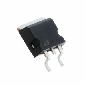
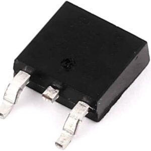
7805ST TO263
The L78 series of three-terminal positive regulators is available in TO-220, TO-220FP, D²PAK and DPAK packages and several fixed output voltages, making it useful in a wide range of applications.
These regulators can provide local on-card regulation, eliminating the distribution problems associated with single point regulation. Each type embeds internal current limiting, thermal shut-down and safe area protection, making it essentially indestructible. If adequate heat sinking is provided, they can deliver over 1 A output current. Although designed primarily as fixed voltage regulators, these devices can be used with external components to obtain adjustable voltage and currents.
7812ST TO263
The L78 series of three-terminal positive regulators is available in TO-220, TO-220FP, D²PAK and DPAK packages and several fixed output voltages, making it useful in a wide range of applications.
These regulators can provide local on-card regulation, eliminating the distribution problems associated with single point regulation. Each type embeds internal current limiting, thermal shut-down and safe area protection, making it essentially indestructible. If adequate heat sinking is provided, they can deliver over 1 A output current. Although designed primarily as fixed voltage regulators, these devices can be used with external components to obtain adjustable voltage and currents.
7815 ST TO263
The L78 series of three-terminal positive regulators is available in TO-220, TO-220FP, D²PAK and DPAK packages and several fixed output voltages, making it useful in a wide range of applications.
These regulators can provide local on-card regulation, eliminating the distribution problems associated with single point regulation. Each type embeds internal current limiting, thermal shut-down and safe area protection, making it essentially indestructible. If adequate heat sinking is provided, they can deliver over 1 A output current. Although designed primarily as fixed voltage regulators, these devices can be used with external components to obtain adjustable voltage and currents.
78L05ST SOIC
The L78L series of three-terminal positive regulators employ internal current limiting and thermal shutdown, making them essentially indestructible. If adequate heat-sink is provided, they can deliver up to 100 mA output current. They are intended as fixed voltage regulators in a wide range of applications including local or on-card regulation for elimination of noise and distribution problems associated with single-point regulation. In addition, they can be used with power pass elements to make high-current voltage regulators. The L78L series used as Zener diode/resistor combination replacement, offers e improvement along with lower quiescent current and lower noise.
78L05ST SOT89
The L78L series of three-terminal positive regulators employ internal current limiting and thermal shutdown, making them essentially indestructible. If adequate heat-sink is provided, they can deliver up to 100 mA output current. They are intended as fixed voltage regulators in a wide range of applications including local or on-card regulation for elimination of noise and distribution problems associated with single-point regulation. In addition, they can be used with power pass elements to make high-current voltage regulators. The L78L series used as Zener diode/resistor combination replacement, offers e improvement along with lower quiescent current and lower noise.
78L12ST SOIC
The L78L series of three-terminal positive regulators employ internal current limiting and thermal shutdown, making them essentially indestructible. If adequate heat-sink is provided, they can deliver up to 100 mA output current. They are intended as fixed voltage regulators in a wide range of applications including local or on-card regulation for elimination of noise and distribution problems associated with single-point regulation. In addition, they can be used with power pass elements to make high-current voltage regulators. The L78L series used as Zener diode/resistor combination replacement, offers e improvement along with lower quiescent current and lower noise.
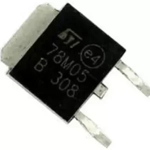
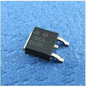
78M05ST DPAK
The L78M series of three-terminal positive regulators is available in TO-220, TO-220FP, DPAK and IPAK packages and with several fixed output voltages, making it useful in a wide range of applications. These regulators can provide local on-card regulation, eliminating the distribution problems associated with single point regulation. Each type employs internal current limiting, thermal shutdown and safe area protection, resulting it essentially indestructible. If adequate heat sinking is provided, they can deliver over 0.5 A output current. Although designed primarily as fixed voltage regulators, these devices can be used with external components to obtain adjustable voltage and currents.
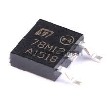
78M12ST DPAK
The L78M series of three-terminal positive regulators is available in TO-220, TO-220FP, DPAK and IPAK packages and with several fixed output voltages, making it useful in a wide range of applications. These regulators can provide local on-card regulation, eliminating the distribution problems associated with single point regulation. Each type employs internal current limiting, thermal shutdown and safe area protection, resulting it essentially indestructible. If adequate heat sinking is provided, they can deliver over 0.5 A output current. Although designed primarily as fixed voltage regulators, these devices can be used with external components to obtain adjustable voltage and currents.
78M15ST DPAK
The L78M series of three-terminal positive regulators is available in TO-220, TO-220FP, DPAK and IPAK packages and with several fixed output voltages, making it useful in a wide range of applications. These regulators can provide local on-card regulation, eliminating the distribution problems associated with single point regulation. Each type employs internal current limiting, thermal shutdown and safe area protection, resulting it essentially indestructible. If adequate heat sinking is provided, they can deliver over 0.5 A output current. Although designed primarily as fixed voltage regulators, these devices can be used with external components to obtain adjustable voltage and currents.
78M18ST DPAK
The L78M series of three-terminal positive regulators is available in TO-220, TO-220FP, DPAK and IPAK packages and with several fixed output voltages, making it useful in a wide range of applications. These regulators can provide local on-card regulation, eliminating the distribution problems associated with single point regulation. Each type employs internal current limiting, thermal shutdown and safe area protection, resulting it essentially indestructible. If adequate heat sinking is provided, they can deliver over 0.5 A output current. Although designed primarily as fixed voltage regulators, these devices can be used with external components to obtain adjustable voltage and currents.
78M24ST DPAK
The L78M series of three-terminal positive regulators is available in TO-220, TO-220FP, DPAK and IPAK packages and with several fixed output voltages, making it useful in a wide range of applications. These regulators can provide local on-card regulation, eliminating the distribution problems associated with single point regulation. Each type employs internal current limiting, thermal shutdown and safe area protection, resulting it essentially indestructible. If adequate heat sinking is provided, they can deliver over 0.5 A output current. Although designed primarily as fixed voltage regulators, these devices can be used with external components to obtain adjustable voltage and currents.
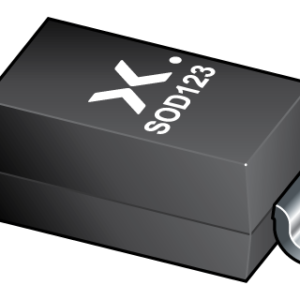
BZT52-C4V7
Single Zener diodes in a SOD123 package
General-purpose Zener diodes in a SOD123 small Surface-Mounted Device (SMD) plastic package.
Features and benefits
- Total power dissipation: ≤ 590 mW
- Wide working voltage range: nominal 2.4 V to 75 V (E24 range)
- Small plastic package suitable for surface-mounted design
- Low differential resistance
- AEC-Q101 qualified
BZT52-C5V1
Single Zener diodes in a SOD123 package
General-purpose Zener diodes in a SOD123 small Surface-Mounted Device (SMD) plastic package.
Features and benefits
- Total power dissipation: ≤ 590 mW
- Wide working voltage range: nominal 2.4 V to 75 V (E24 range)
- Small plastic package suitable for surface-mounted design
- Low differential resistance
- AEC-Q101 qualified
BZT52-C5V6
Single Zener diodes in a SOD123 package
General-purpose Zener diodes in a SOD123 small Surface-Mounted Device (SMD) plastic package.
Features and benefits
- Total power dissipation: ≤ 590 mW
- Wide working voltage range: nominal 2.4 V to 75 V (E24 range)
- Small plastic package suitable for surface-mounted design
- Low differential resistance
- AEC-Q101 qualified

BZT52-H6V2
Single Zener diodes in a SOD123 package
General-purpose Zener diodes in a SOD123 small Surface-Mounted Device (SMD) plastic package.
Features and benefits
- Total power dissipation: ≤ 830 mW
- Low differential resistance
- Wide working voltage range: nominal 2.4 V to 75 V (E24 range)
- AEC-Q101 qualified
- Small plastic package suitable for surface-mounted design

BZT52H-24
General-purpose Zener diodes in a SOD123F small and flat lead Surface-Mounted Device (SMD) plastic package.
Features and benefits
- Total power dissipation: ≤ 830 mW
- Low differential resistance
- Wide working voltage range: nominal 2.4 V to 75 V (E24 range)
- AEC-Q101 qualified
- Small plastic package suitable for surface-mounted design
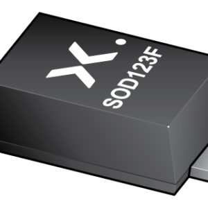
BZT52H-C10
Single Zener diodes in a SOD123F package
General-purpose Zener diodes in a SOD123F small and flat lead Surface-Mounted Device (SMD) plastic package.
Features and benefits
- Total power dissipation: ≤ 830 mW
- Low differential resistance
- Wide working voltage range: nominal 2.4 V to 75 V (E24 range)
- AEC-Q101 qualified
- Small plastic package suitable for surface-mounted design
BZT52H-C12
General-purpose Zener diodes in a SOD123F small and flat lead Surface-Mounted Device (SMD) plastic package.
Features and benefits
- Total power dissipation: ≤ 830 mW
- Low differential resistance
- Wide working voltage range: nominal 2.4 V to 75 V (E24 range)
- AEC-Q101 qualified
- Small plastic package suitable for surface-mounted design