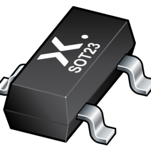
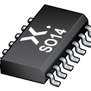
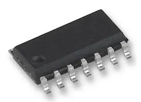
74HC00D
Quad 2-input NAND gate
Features and benefits- Total power dissipation: ≤ 590 mW
- Wide working voltage range: nominal 2.4 V to 75 V (E24 range)
- Small plastic package s
- Wide supply voltage range from 2.0 to 6.0 V
- CMOS low power dissipation
- High noise immunity
- Latch-up performance exceeds 100 mA per JESD 78 Class II Level B
- Input levels:
- For 74HC00: CMOS level
- For 74HCT00: TTL level
- Complies with JEDEC standards:
- JESD8C (2.7 V to 3.6 V)
- JESD7A (2.0 V to 6.0 V)
- ESD protection:
- HBM JESD22-A114F exceeds 2000 V
- MM JESD22-A115-A exceeds 200 V
- Multiple package options
- Specified from -40 °C to +85 °C and from -40 °C to +125 °C
- uitable for surface-mounted design
- Low differential resistance
- AEC-Q101 qualified
74HC02D
Quad 2-input NOR gate
Features and benefits- Wide supply voltage range from 2.0 V to 6.0 V
- CMOS low power dissipation
- High noise immunity
- Latch-up performance exceeds 100 mA per JESD 78 Class II Level B
- Input levels:
- For 74HC02: CMOS level
- For 74HCT02: TTL level
- Complies with JEDEC standards:
- JESD8C (2.7 V to 3.6 V)
- JESD7A (2.0 V to 6.0 V)
- ESD protection:
- HBM JESD22-A114F exceeds 2000 V
- MM JESD22-A115-A exceeds 200 V
- Multiple package options
- Specified from -40 °C to +85 °C and from -40 °C to +125 °C
74HC04D
Hex inverter
Features and benefits- Wide supply voltage range from 2.0 V to 6.0 V
- CMOS low power dissipation
- High noise immunity
- Latch-up performance exceeds 100 mA per JESD 78 Class II Level B
- Complies with JEDEC standards:
- JESD8C (2.7 V to 3.6 V)
- JESD7A (2.0 V to 6.0 V)
- Input levels:
- For 74HC04: CMOS level
- For 74HCT04: TTL level
- ESD protection:
- HBM JESD22-A114F exceeds 2000 V
- MM JESD22-A115-A exceeds 200 V
- Multiple package options
- Specified from -40 °C to +85 °C and from -40 °C to +125 °C
74HC08D
Quad 2-input AND gate
Features and benefits- Wide supply voltage range from 2.0 V to 6.0 V
- CMOS low power dissipation
- High noise immunity
- Latch-up performance exceeds 100 mA per JESD 78 Class II Level B
- Input levels:
- For 74HC08: CMOS level
- For 74HCT08: TTL level
- Complies with JEDEC standards:
- JESD8C (2.7 V to 3.6 V)
- JESD7A (2.0 V to 6.0 V)
- ESD protection:
- HBM JESD22-A114F exceeds 2000 V
- MM JESD22-A115-A exceeds 200 V
- Multiple package options
- Specified from -40 °C to +85 °C and from -40 °C to +125 °C
74HC125D
Quad buffer/line driver; 3-state
Features and benefits- Wide supply voltage range from 2.0 to 6.0 V
- CMOS low power dissipation
- High noise immunity
- Latch-up performance exceeds 100 mA per JESD 78 Class II Level B
- Complies with JEDEC standards:
- JESD8C (2.7 V to 3.6 V)
- JESD7A (2.0 V to 6.0 V)
- Input levels:
- The 74HC125: CMOS levels
- The 74HCT125: TTL levels
- ESD protection:
- HBM JESD22-A114F exceeds 2000 V
- MM JESD22-A115-A exceeds 200 V
- Specified from -40 °C to +85 °C and from -40 °C to +125 °C
74HC126D
Quad buffer/line driver; 3-state
Features and benefits- Wide supply voltage range from 2.0 to 6.0 V
- CMOS low power dissipation
- High noise immunity
- Latch-up performance exceeds 100 mA per JESD 78 Class II Level B
- Inverting outputs
- Complies with JEDEC standards:
- JESD8C (2.7 V to 3.6 V)
- JESD7A (2.0 V to 6.0 V)
- Input levels:
- For 74HC126: CMOS levels
- For 74HCT126: TTL levels
- ESD protection:
- HBM JESD22-A114F exceeds 2000 V
- MM JESD22-A115-A exceeds 200 V
- Specified from -40 °C to +85 °C and from -40 °C to +125 °C
74HC132D
Quad 2-input NAND Schmitt trigger
Features and benefits- Wide supply voltage range from 2.0 to 6.0 V
- CMOS low power dissipation
- High noise immunity
- Unlimited input rise and fall times
- Latch-up performance exceeds 100 mA per JESD 78 Class II Level B
- Complies with JEDEC standards:
- JESD8C (2.7 V to 3.6 V)
- JESD7A (2.0 V to 6.0 V)
- ESD protection:
- HBM JESD22-A114F exceeds 2000 V
- MM JESD22-A115-A exceeds 200 V
- Multiple package options
- Specified from −40 °C to +85 °C and from −40 °C to +125 °C
74HC132ST SOIC
The M74HC132 is a high-speed CMOS quad 2-input Schmitt NAND gate fabricated with silicon gate C2MOS technology. Pin configuration and function are identical to those of the M74HC00. The hysteresis characteristics (around 20 % VCC) of all inputs allow slowly changing input signals to be transformed into sharply defined jitter-free output signals.
All inputs are equipped with protection circuits against static discharge and transient excess voltage.
Download Datasheet:


