

Find Special Offers Daily From SMD Electro. Hurry as this is for limited period only
SPECIAL OFFERS
10
Feb
ALL FOR EDSM
USB6B1ST SOIC
In order to prevent fast transients from leading to severe damages in a high speed data system, a specific protection has been developed by STMicroelectronics.
The USB6B1 protects the two input lines against overvoltage. Besides, this device also keeps the power rails in a safe limit thanks to the integrated Transil diode.
ULQ2003ST SOIC
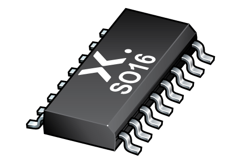
The ULQ2001, ULQ2003 and ULQ2004 are high voltage, high current Darlington arrays each containing seven open collector Darlington pairs with common emitters. Each channel rated at 500 mA and can withstand peak currents of 600 mA. Suppression diodes are included for inductive load driving and the inputs are pinned opposite the outputs to simplify board layout. The versions interface to all common logic families. These versatile devices are useful for driving a wide range of loads including solenoids, relays DC motors, LED displays filament lamps, thermal print-heads and high power buffers. The ULQ2001A/2003A and 2004A are supplied in 16 pin plastic DIP packages with a copper lead-frame to reduce thermal resistance. They are available also in small outline package (SO16) as ULQ2003D1/2004D1. The ULQ2003 is available as Automotive Grade in SO16 package. The commercial part numbers is shown in the order codes. This device is qualified according to the specification AEC-Q100 of the Automotive market, in the temperature range -40 °C to 125 °C and the statistical tests PAT, SYL, SBL are performed.
ULN2003ST SOIC
The ULN2001, ULN2002, ULN2003 and ULN 2004 are high-voltage, high-current Darlington arrays each containing seven open collector Darlington pairs with common emitters. Each channel is rated at 500 mA and can withstand peak currents of 600 mA. Suppression diodes are included for inductive load driving and the inputs are pinned opposite the outputs to simplify board layout.
The versions interface to all common logic families: ULN2001 (general purpose, DTL, TTL, PMOS, CMOS); ULN2002 (14 - 25 V PMOS); ULN2003 (5 V TTL, CMOS); ULN2004 (6 - 15 V CMOS, PMOS).
These versatile devices are useful for driving a wide range of loads including solenoids, relay DC motors, LED display filament lamps, thermal printheads and high-power buffers.
The ULN2001A/2002A/2003A and 2004A are supplied in a 16-pin DIP package with a copper leadframe to reduce thermal resistance. They are available also in small outline package (SO-16) as ULN2001D1/2002D1/2003D1/ 2004D1.
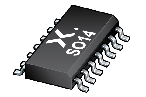
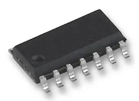
UC3845ST SOIC14
The UC284xB family of control ICs provides the necessary features to implement off-line or DC to DC fixed frequency current mode control schemes with a minimal external parts count. Internally implemented circuits include a trimmed oscillator for precise DUTY CYCLE CONTROL under voltage lockout featuring start-up current less than 0.5mA, a precision reference trimmed for accuracy at the error amp input, logic to insure latched operation, a PWM comparator which also provides current limit control, and a totem pole output stage designed to source or sink high peak current. The output stage, suitable for driving N-Channel MOSFETs, is low in the off-state.
Differences between members of this family are the under-voltage lockout thresholds and maximum duty cycle ranges. The UC2842B and UC2844B have UVLO thresholds of 16V (on) and 10V (off), ideally suited off-line applications The corresponding thresholds for the UC2843B and UC2845B are 8.5V and 7.9V. The UC2842B and UC2843B can operate to duty cycles approaching 100%. A range of the zero to < 50 % is obtained by the UC2844B and UC2845B by the addition of an internal toggle flip flop which blanks the output off every other clock cycle.
VERSIONS HAVE EVOLVED OVER THE YEARS
Find your Component here
Search By Part No, SKU, Company name, country, brand Ect.
latest Components
Featured Products
Will your clients accept that you go about things order.
2N7002
74HC00D
Quad 2-input NAND gate
The 74HC00; 74HCT00 is a quad 2-input NAND gate. Inputs include clamp diodes. This enables the use of current limiting resistors to interface inputs to voltages in excess of VCC.
Features and benefits
- Total power dissipation: ≤ 590 mW
- Wide working voltage range: nominal 2.4 V to 75 V (E24 range)
- Small plastic package s
- Wide supply voltage range from 2.0 to 6.0 V
- CMOS low power dissipation
- High noise immunity
- Latch-up performance exceeds 100 mA per JESD 78 Class II Level B
- Input levels:
- For 74HC00: CMOS level
- For 74HCT00: TTL level
- Complies with JEDEC standards:
- JESD8C (2.7 V to 3.6 V)
- JESD7A (2.0 V to 6.0 V)
- ESD protection:
- HBM JESD22-A114F exceeds 2000 V
- MM JESD22-A115-A exceeds 200 V
- Multiple package options
- Specified from -40 °C to +85 °C and from -40 °C to +125 °C
- uitable for surface-mounted design
- Low differential resistance
- AEC-Q101 qualified
74HC02D
Quad 2-input NOR gate
The 74HC02; 74HCT02 is a quad 2-input NOR gate. Inputs include clamp diodes. This enables the use of current limiting resistors to interface inputs to voltages in excess of VCC.
Features and benefits
- Wide supply voltage range from 2.0 V to 6.0 V
- CMOS low power dissipation
- High noise immunity
- Latch-up performance exceeds 100 mA per JESD 78 Class II Level B
- Input levels:
- For 74HC02: CMOS level
- For 74HCT02: TTL level
- Complies with JEDEC standards:
- JESD8C (2.7 V to 3.6 V)
- JESD7A (2.0 V to 6.0 V)
- ESD protection:
- HBM JESD22-A114F exceeds 2000 V
- MM JESD22-A115-A exceeds 200 V
- Multiple package options
- Specified from -40 °C to +85 °C and from -40 °C to +125 °C
74HC04D
Hex inverter
The 74HC04; 74HCT04 is a hex inverter. The inputs include clamp diodes that enable the use of current limiting resistors to interface inputs to voltages in excess of VCC.
Features and benefits
- Wide supply voltage range from 2.0 V to 6.0 V
- CMOS low power dissipation
- High noise immunity
- Latch-up performance exceeds 100 mA per JESD 78 Class II Level B
- Complies with JEDEC standards:
- JESD8C (2.7 V to 3.6 V)
- JESD7A (2.0 V to 6.0 V)
- Input levels:
- For 74HC04: CMOS level
- For 74HCT04: TTL level
- ESD protection:
- HBM JESD22-A114F exceeds 2000 V
- MM JESD22-A115-A exceeds 200 V
- Multiple package options
- Specified from -40 °C to +85 °C and from -40 °C to +125 °C
74HC08D
Quad 2-input AND gate
The 74HC08; 74HCT08 is a quad 2-input AND gate. Inputs include clamp diodes. This enables the use of current limiting resistors to interface inputs to voltages in excess of VCC.
Features and benefits
- Wide supply voltage range from 2.0 V to 6.0 V
- CMOS low power dissipation
- High noise immunity
- Latch-up performance exceeds 100 mA per JESD 78 Class II Level B
- Input levels:
- For 74HC08: CMOS level
- For 74HCT08: TTL level
- Complies with JEDEC standards:
- JESD8C (2.7 V to 3.6 V)
- JESD7A (2.0 V to 6.0 V)
- ESD protection:
- HBM JESD22-A114F exceeds 2000 V
- MM JESD22-A115-A exceeds 200 V
- Multiple package options
- Specified from -40 °C to +85 °C and from -40 °C to +125 °C
74HC125D
Quad buffer/line driver; 3-state
The 74HC125; 74HCT125 is a quad buffer/line driver with 3-state outputs controlled by the output enable inputs (nOE). A HIGH on nOE causes the outputs to assume a high impedance OFF-state. Inputs include clamp diodes. This enables the use of current limiting resistors to interface inputs to voltages in excess of VCC.
Features and benefits
- Wide supply voltage range from 2.0 to 6.0 V
- CMOS low power dissipation
- High noise immunity
- Latch-up performance exceeds 100 mA per JESD 78 Class II Level B
- Complies with JEDEC standards:
- JESD8C (2.7 V to 3.6 V)
- JESD7A (2.0 V to 6.0 V)
- Input levels:
- The 74HC125: CMOS levels
- The 74HCT125: TTL levels
- ESD protection:
- HBM JESD22-A114F exceeds 2000 V
- MM JESD22-A115-A exceeds 200 V
- Specified from -40 °C to +85 °C and from -40 °C to +125 °C
74HC126D
Quad buffer/line driver; 3-state
The 74HC126; 74HCT126 is a quad buffer/line driver with 3-state outputs controlled by the output enable inputs (nOE). A LOW on nOE causes the outputs to assume a high-impedance OFF-state. Inputs include clamp diodes. This enables the use of current limiting resistors to interface inputs to voltages in excess of VCC.
Features and benefits
- Wide supply voltage range from 2.0 to 6.0 V
- CMOS low power dissipation
- High noise immunity
- Latch-up performance exceeds 100 mA per JESD 78 Class II Level B
- Inverting outputs
- Complies with JEDEC standards:
- JESD8C (2.7 V to 3.6 V)
- JESD7A (2.0 V to 6.0 V)
- Input levels:
- For 74HC126: CMOS levels
- For 74HCT126: TTL levels
- ESD protection:
- HBM JESD22-A114F exceeds 2000 V
- MM JESD22-A115-A exceeds 200 V
- Specified from -40 °C to +85 °C and from -40 °C to +125 °C
74HC132D
Quad 2-input NAND Schmitt trigger
The 74HC132; 74HCT132 is a quad 2-input NAND gate with Schmitt-trigger inputs. Inputs include clamp diodes. This enables the use of current limiting resistors to interface inputs to voltages in excess of VCC. Schmitt trigger inputs transform slowly changing input signals into sharply defined jitter-free output signals.
Features and benefits
- Wide supply voltage range from 2.0 to 6.0 V
- CMOS low power dissipation
- High noise immunity
- Unlimited input rise and fall times
- Latch-up performance exceeds 100 mA per JESD 78 Class II Level B
- Complies with JEDEC standards:
- JESD8C (2.7 V to 3.6 V)
- JESD7A (2.0 V to 6.0 V)
- ESD protection:
- HBM JESD22-A114F exceeds 2000 V
- MM JESD22-A115-A exceeds 200 V
- Multiple package options
- Specified from −40 °C to +85 °C and from −40 °C to +125 °C
74HC132ST SOIC
The M74HC132 is a high-speed CMOS quad 2-input Schmitt NAND gate fabricated with silicon gate C2MOS technology. Pin configuration and function are identical to those of the M74HC00. The hysteresis characteristics (around 20 % VCC) of all inputs allow slowly changing input signals to be transformed into sharply defined jitter-free output signals.
All inputs are equipped with protection circuits against static discharge and transient excess voltage.
Download Datasheet:
74HC138D
3-to-8 line decoder/demultiplexer; inverting
The 74HC138; 74HCT138 decodes three binary weighted address inputs (A0, A1 and A2) to eight mutually exclusive outputs (Y0 to Y7). The device features three enable inputs (E1, E2 and E3). Every output will be HIGH unless E1 and E2 are LOW and E3 is HIGH. This multiple enable function allows easy parallel expansion to a 1-of-32 (5 to 32 lines) decoder with just four '138 ICs and one inverter. The '138 can be used as an eight output demultiplexer by using one of the active LOW enable inputs as the data input and the remaining enable inputs as strobes. Inputs include clamp diodes. This enables the use of current limiting resistors to interface inputs to voltages in excess of VCC.
Features and benefits
- Wide supply voltage range from 2.0 to 6.0 V
- CMOS low power dissipation
- High noise immunity
- Latch-up performance exceeds 100 mA per JESD 78 Class II Level B
- Demultiplexing capability
- Multiple input enable for easy expansion
- Ideal for memory chip select decoding
- Active LOW mutually exclusive outputs
- Input levels:
- For 74HC138: CMOS level
- For 74HCT138: TTL level
- Complies with JEDEC standards:
- JESD8C (2.7 V to 3.6 V)
- JESD7A (2.0 V to 6.0 V)
- ESD protection:
- HBM JESD22-A114F exceeds 2000 V
- MM JESD22-A115-A exceeds 200 V
- Multiple package options
- Specified from -40 °C to +85 °C and from -40 °C to +125 °C
Load more products
Loading...
Products On offer
25M+
Countries supported
46
Currency supported
68
Stock Availablity
24/7
GLOBAL SUPPLIERS
One of the largest Electronics Component Distributor.
One morning, when Gregor Samsa woke from troubled dreams, he found himself transformed in his bed into a horrible vermin. He lay on his armour-like back, and if he lifted his head a little he could see his brown belly.

