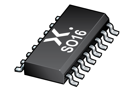
74HC151D
8-input multiplexer
The 74HC151; 74HCT151 are 8-bit multiplexer with eight binary inputs (I0 to I7), three select inputs (S0 to S2) and an enable input (E). One of the eight binary inputs is selected by the select inputs and routed to the complementary outputs (Y and Y). A HIGH on E forces the output Y LOW and output Y HIGH. Inputs also include clamp diodes that enable the use of current limiting resistors to interface inputs to voltages in excess of VCC.
Features and benefits
- Specified in compliance with JEDEC standard no. 7A
- Input levels:
- For 74HC151: CMOS level
- For 74HCT151: TTL level
- Low-power dissipation
- Non-inverting data path
- ESD protection:
-
- HBM JESD22-A114F exceeds 2000 V
- MM JESD22-A115-A exceeds 200 V
- Specified from -40 °C to +85 °C and from -40 °C to +125 °C
DOWNLOADS:
SKU:
74HC151NXP SOIC
Category: Analog & Logic ICs
Shipping & Delivery
Related products
74HC02D
Quad 2-input NOR gate
The 74HC02; 74HCT02 is a quad 2-input NOR gate. Inputs include clamp diodes. This enables the use of current limiting resistors to interface inputs to voltages in excess of VCC.
Features and benefits
- Wide supply voltage range from 2.0 V to 6.0 V
- CMOS low power dissipation
- High noise immunity
- Latch-up performance exceeds 100 mA per JESD 78 Class II Level B
- Input levels:
- For 74HC02: CMOS level
- For 74HCT02: TTL level
- Complies with JEDEC standards:
- JESD8C (2.7 V to 3.6 V)
- JESD7A (2.0 V to 6.0 V)
- ESD protection:
- HBM JESD22-A114F exceeds 2000 V
- MM JESD22-A115-A exceeds 200 V
- Multiple package options
- Specified from -40 °C to +85 °C and from -40 °C to +125 °C
74HC04D
Hex inverter
The 74HC04; 74HCT04 is a hex inverter. The inputs include clamp diodes that enable the use of current limiting resistors to interface inputs to voltages in excess of VCC.
Features and benefits
- Wide supply voltage range from 2.0 V to 6.0 V
- CMOS low power dissipation
- High noise immunity
- Latch-up performance exceeds 100 mA per JESD 78 Class II Level B
- Complies with JEDEC standards:
- JESD8C (2.7 V to 3.6 V)
- JESD7A (2.0 V to 6.0 V)
- Input levels:
- For 74HC04: CMOS level
- For 74HCT04: TTL level
- ESD protection:
- HBM JESD22-A114F exceeds 2000 V
- MM JESD22-A115-A exceeds 200 V
- Multiple package options
- Specified from -40 °C to +85 °C and from -40 °C to +125 °C
74HC08D
Quad 2-input AND gate
The 74HC08; 74HCT08 is a quad 2-input AND gate. Inputs include clamp diodes. This enables the use of current limiting resistors to interface inputs to voltages in excess of VCC.
Features and benefits
- Wide supply voltage range from 2.0 V to 6.0 V
- CMOS low power dissipation
- High noise immunity
- Latch-up performance exceeds 100 mA per JESD 78 Class II Level B
- Input levels:
- For 74HC08: CMOS level
- For 74HCT08: TTL level
- Complies with JEDEC standards:
- JESD8C (2.7 V to 3.6 V)
- JESD7A (2.0 V to 6.0 V)
- ESD protection:
- HBM JESD22-A114F exceeds 2000 V
- MM JESD22-A115-A exceeds 200 V
- Multiple package options
- Specified from -40 °C to +85 °C and from -40 °C to +125 °C
74HC125D
Quad buffer/line driver; 3-state
The 74HC125; 74HCT125 is a quad buffer/line driver with 3-state outputs controlled by the output enable inputs (nOE). A HIGH on nOE causes the outputs to assume a high impedance OFF-state. Inputs include clamp diodes. This enables the use of current limiting resistors to interface inputs to voltages in excess of VCC.
Features and benefits
- Wide supply voltage range from 2.0 to 6.0 V
- CMOS low power dissipation
- High noise immunity
- Latch-up performance exceeds 100 mA per JESD 78 Class II Level B
- Complies with JEDEC standards:
- JESD8C (2.7 V to 3.6 V)
- JESD7A (2.0 V to 6.0 V)
- Input levels:
- The 74HC125: CMOS levels
- The 74HCT125: TTL levels
- ESD protection:
- HBM JESD22-A114F exceeds 2000 V
- MM JESD22-A115-A exceeds 200 V
- Specified from -40 °C to +85 °C and from -40 °C to +125 °C
74HC126D
Quad buffer/line driver; 3-state
The 74HC126; 74HCT126 is a quad buffer/line driver with 3-state outputs controlled by the output enable inputs (nOE). A LOW on nOE causes the outputs to assume a high-impedance OFF-state. Inputs include clamp diodes. This enables the use of current limiting resistors to interface inputs to voltages in excess of VCC.
Features and benefits
- Wide supply voltage range from 2.0 to 6.0 V
- CMOS low power dissipation
- High noise immunity
- Latch-up performance exceeds 100 mA per JESD 78 Class II Level B
- Inverting outputs
- Complies with JEDEC standards:
- JESD8C (2.7 V to 3.6 V)
- JESD7A (2.0 V to 6.0 V)
- Input levels:
- For 74HC126: CMOS levels
- For 74HCT126: TTL levels
- ESD protection:
- HBM JESD22-A114F exceeds 2000 V
- MM JESD22-A115-A exceeds 200 V
- Specified from -40 °C to +85 °C and from -40 °C to +125 °C
74HC165D
8-bit parallel-in/serial out shift register
The 74HC165; 74HCT165 are 8-bit serial or parallel-in/serial-out shift registers. The device features a serial data input (DS), eight parallel data inputs (D0 to D7) and two complementary serial outputs (Q7 and Q7). When the parallel load input (PL) is LOW the data from D0 to D7 is loaded into the shift register asynchronously. When PL is HIGH data enters the register serially at DS. When the clock enable input (CE) is LOW data is shifted on the LOW-to-HIGH transitions of the CP input. A HIGH on CE will disable the CP input. Inputs are overvoltage tolerant to 15 V. This enables the device to be used in HIGH-to-LOW level shifting applications.
Features and benefits
- Wide supply voltage range from 2.0 to 6.0 V
- CMOS low power dissipation
- High noise immunity
- Latch-up performance exceeds 100 mA per JESD 78 Class II Level B
- Asynchronous 8-bit parallel load
- Synchronous serial input
- Input levels:
- For 74HC165: CMOS level
- For 74HCT165: TTL level
- Complies with JEDEC standards:
- JESD8C (2.7 V to 3.6 V)
- JESD7A (2.0 V to 6.0 V)
- ESD protection:
- HBM JESD22-A114F exceeds 2000 V
- MM JESD22-A115-A exceeds 200 V
- Multiple package options
- Specified from -40 °C to +85 °C and from -40 °C to +125 °C
74HC238D
3-to-8 line decoder/demultiplexer
The 74HC238; 74HCT238 decodes three binary weighted address inputs (A0, A1 and A2) to eight mutually exclusive outputs (Y0 to Y7). The device features three enable inputs (E1 and E2 and E3). Every output will be LOW unless E1 and E2 are LOW and E3 is HIGH. This multiple enable function allows easy parallel expansion to a 1-of-32 (5 to 32 lines) decoder with just four '238 ICs and one inverter. The '238 can be used as an eight output demultiplexer by using one of the active LOW enable inputs as the data input and the remaining enable inputs as strobes. Inputs include clamp diodes. This enables the use of current limiting resistors to interface inputs to voltages in excess of VCC.
Features and benefits
- Wide supply voltage range from 2.0 to 6.0 V
- CMOS low power dissipation
- High noise immunity
- Demultiplexing capability
- Multiple input enable for easy expansion
- Ideal for memory chip select decoding
- Active HIGH mutually exclusive outputs
- Input levels:
- For 74HC238: CMOS level
- For 74HCT238: TTL level
- Complies with JEDEC standards
- JESD8C (2.7 V to 3.6 V)
- JESD7A (2.0 V to 6.0 V)
- Latch-up performance exceeds 100 mA per JESD 78 Class II Level B
- ESD protection:
- HBM JESD22-A114F exceeds 2000 V
- MM JESD22-A115-A exceeds 200 V
- Multiple package options
- Specified from -40 °C to +85 °C and from -40 °C to +125 °C
74HC245D
Octal bus transceiver; 3-state
The 74HC245; 74HCT245 is an 8-bit transceiver with 3-state outputs. The device features an output enable (OE) and send/receive (DIR) for direction control. A HIGH on OE causes the outputs to assume a high-impedance OFF-state. Inputs include clamp diodes. This enables the use of current limiting resistors to interface inputs to voltages in excess of VCC.
Features and benefits
- Wide supply voltage range from 2.0 to 6.0 V
- CMOS low power dissipation
- High noise immunity
- Octal bidirectional bus interface
- Non-inverting 3-state outputs
- Input levels:
- For 74HC245: CMOS level
- For 74HCT245: TTL level
- Complies with JEDEC standards
- JESD8C (2.7 V to 3.6 V)
- JESD7A (2.0 V to 6.0 V)
- Latch-up performance exceeds 100 mA per JESD 78 Class II Level B
- ESD protection:
-
- HBM JESD22-A114F exceeds 2000 V
- MM JESD22-A115-A exceeds 200 V
- Multiple package options
- Specified from -40 °C to +85 °C and from -40 °C to +125 °C


