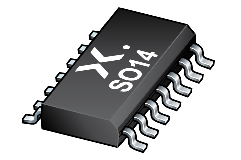
74HC04D
Hex inverter
The 74HC04; 74HCT04 is a hex inverter. The inputs include clamp diodes that enable the use of current limiting resistors to interface inputs to voltages in excess of VCC.
Features and benefits
- Wide supply voltage range from 2.0 V to 6.0 V
- CMOS low power dissipation
- High noise immunity
- Latch-up performance exceeds 100 mA per JESD 78 Class II Level B
- Complies with JEDEC standards:
- JESD8C (2.7 V to 3.6 V)
- JESD7A (2.0 V to 6.0 V)
- Input levels:
- For 74HC04: CMOS level
- For 74HCT04: TTL level
- ESD protection:
- HBM JESD22-A114F exceeds 2000 V
- MM JESD22-A115-A exceeds 200 V
- Multiple package options
- Specified from -40 °C to +85 °C and from -40 °C to +125 °C
DOWNLOADS:
SKU:
74HC04NXP SOIC
Category: Analog & Logic ICs
Shipping & Delivery
Related products
74HC00D
Quad 2-input NAND gate
The 74HC00; 74HCT00 is a quad 2-input NAND gate. Inputs include clamp diodes. This enables the use of current limiting resistors to interface inputs to voltages in excess of VCC.
Features and benefits
- Total power dissipation: ≤ 590 mW
- Wide working voltage range: nominal 2.4 V to 75 V (E24 range)
- Small plastic package s
- Wide supply voltage range from 2.0 to 6.0 V
- CMOS low power dissipation
- High noise immunity
- Latch-up performance exceeds 100 mA per JESD 78 Class II Level B
- Input levels:
- For 74HC00: CMOS level
- For 74HCT00: TTL level
- Complies with JEDEC standards:
- JESD8C (2.7 V to 3.6 V)
- JESD7A (2.0 V to 6.0 V)
- ESD protection:
- HBM JESD22-A114F exceeds 2000 V
- MM JESD22-A115-A exceeds 200 V
- Multiple package options
- Specified from -40 °C to +85 °C and from -40 °C to +125 °C
- uitable for surface-mounted design
- Low differential resistance
- AEC-Q101 qualified
74HC02D
Quad 2-input NOR gate
The 74HC02; 74HCT02 is a quad 2-input NOR gate. Inputs include clamp diodes. This enables the use of current limiting resistors to interface inputs to voltages in excess of VCC.
Features and benefits
- Wide supply voltage range from 2.0 V to 6.0 V
- CMOS low power dissipation
- High noise immunity
- Latch-up performance exceeds 100 mA per JESD 78 Class II Level B
- Input levels:
- For 74HC02: CMOS level
- For 74HCT02: TTL level
- Complies with JEDEC standards:
- JESD8C (2.7 V to 3.6 V)
- JESD7A (2.0 V to 6.0 V)
- ESD protection:
- HBM JESD22-A114F exceeds 2000 V
- MM JESD22-A115-A exceeds 200 V
- Multiple package options
- Specified from -40 °C to +85 °C and from -40 °C to +125 °C
74HC08D
Quad 2-input AND gate
The 74HC08; 74HCT08 is a quad 2-input AND gate. Inputs include clamp diodes. This enables the use of current limiting resistors to interface inputs to voltages in excess of VCC.
Features and benefits
- Wide supply voltage range from 2.0 V to 6.0 V
- CMOS low power dissipation
- High noise immunity
- Latch-up performance exceeds 100 mA per JESD 78 Class II Level B
- Input levels:
- For 74HC08: CMOS level
- For 74HCT08: TTL level
- Complies with JEDEC standards:
- JESD8C (2.7 V to 3.6 V)
- JESD7A (2.0 V to 6.0 V)
- ESD protection:
- HBM JESD22-A114F exceeds 2000 V
- MM JESD22-A115-A exceeds 200 V
- Multiple package options
- Specified from -40 °C to +85 °C and from -40 °C to +125 °C
74HC126D
Quad buffer/line driver; 3-state
The 74HC126; 74HCT126 is a quad buffer/line driver with 3-state outputs controlled by the output enable inputs (nOE). A LOW on nOE causes the outputs to assume a high-impedance OFF-state. Inputs include clamp diodes. This enables the use of current limiting resistors to interface inputs to voltages in excess of VCC.
Features and benefits
- Wide supply voltage range from 2.0 to 6.0 V
- CMOS low power dissipation
- High noise immunity
- Latch-up performance exceeds 100 mA per JESD 78 Class II Level B
- Inverting outputs
- Complies with JEDEC standards:
- JESD8C (2.7 V to 3.6 V)
- JESD7A (2.0 V to 6.0 V)
- Input levels:
- For 74HC126: CMOS levels
- For 74HCT126: TTL levels
- ESD protection:
- HBM JESD22-A114F exceeds 2000 V
- MM JESD22-A115-A exceeds 200 V
- Specified from -40 °C to +85 °C and from -40 °C to +125 °C
74HC138D
3-to-8 line decoder/demultiplexer; inverting
The 74HC138; 74HCT138 decodes three binary weighted address inputs (A0, A1 and A2) to eight mutually exclusive outputs (Y0 to Y7). The device features three enable inputs (E1, E2 and E3). Every output will be HIGH unless E1 and E2 are LOW and E3 is HIGH. This multiple enable function allows easy parallel expansion to a 1-of-32 (5 to 32 lines) decoder with just four '138 ICs and one inverter. The '138 can be used as an eight output demultiplexer by using one of the active LOW enable inputs as the data input and the remaining enable inputs as strobes. Inputs include clamp diodes. This enables the use of current limiting resistors to interface inputs to voltages in excess of VCC.
Features and benefits
- Wide supply voltage range from 2.0 to 6.0 V
- CMOS low power dissipation
- High noise immunity
- Latch-up performance exceeds 100 mA per JESD 78 Class II Level B
- Demultiplexing capability
- Multiple input enable for easy expansion
- Ideal for memory chip select decoding
- Active LOW mutually exclusive outputs
- Input levels:
- For 74HC138: CMOS level
- For 74HCT138: TTL level
- Complies with JEDEC standards:
- JESD8C (2.7 V to 3.6 V)
- JESD7A (2.0 V to 6.0 V)
- ESD protection:
- HBM JESD22-A114F exceeds 2000 V
- MM JESD22-A115-A exceeds 200 V
- Multiple package options
- Specified from -40 °C to +85 °C and from -40 °C to +125 °C
74HC14D
Hex inverting Schmitt trigger
The 74HC14; 74HCT14 is a hex inverter with Schmitt-trigger inputs. This device features reduced input threshold levels to allow interfacing to TTL logic levels. Inputs also include clamp diodes, this enables the use of current limiting resistors to interface inputs to voltages in excess of VCC. Schmitt trigger inputs transform slowly changing input signals into sharply defined jitter-free output signals.
Features and benefits
- Wide supply voltage range from 2.0 to 6.0 V
- CMOS low power dissipation
- High noise immunity
- Unlimited input rise and fall times
- Latch-up performance exceeds 100 mA per JESD 78 Class II Level B
- Complies with JEDEC standards:
- JESD8C (2.7 V to 3.6 V)
- JESD7A (2.0 V to 6.0 V)
- ESD protection:
- HBM JESD22-A114F exceeds 2000 V
- MM JESD22-A115-A exceeds 200 V
- Multiple package options
- Specified from -40 °C to +85 °C and from -40 °C to +125 °C
74HC151D
8-input multiplexer
The 74HC151; 74HCT151 are 8-bit multiplexer with eight binary inputs (I0 to I7), three select inputs (S0 to S2) and an enable input (E). One of the eight binary inputs is selected by the select inputs and routed to the complementary outputs (Y and Y). A HIGH on E forces the output Y LOW and output Y HIGH. Inputs also include clamp diodes that enable the use of current limiting resistors to interface inputs to voltages in excess of VCC.
Features and benefits
- Specified in compliance with JEDEC standard no. 7A
- Input levels:
- For 74HC151: CMOS level
- For 74HCT151: TTL level
- Low-power dissipation
- Non-inverting data path
- ESD protection:
-
- HBM JESD22-A114F exceeds 2000 V
- MM JESD22-A115-A exceeds 200 V
- Specified from -40 °C to +85 °C and from -40 °C to +125 °C
74HC164D
8-bit serial-in, parallel-out shift register
The 74HC164; 74HCT164 is an 8-bit serial-in/parallel-out shift register. The device features two serial data inputs (DSA and DSB), eight parallel data outputs (Q0 to Q7). Data is entered serially through DSA or DSB and either input can be used as an active HIGH enable for data entry through the other input. Data is shifted on the LOW-to-HIGH transitions of the clock (CP) input. A LOW on the master reset input (MR) clears the register and forces all outputs LOW, independently of other inputs. Inputs include clamp diodes. This enables the use of current limiting resistors to interface inputs to voltages in excess of VCC.
Features and benefits
- Wide supply voltage range from 2.0 to 6.0 V
- CMOS low power dissipation
- High noise immunity
- Input levels:
- For 74HC164: CMOS level
- For 74HCT164: TTL level
- Gated serial data inputs
- Asynchronous master reset
- Complies with JEDEC standards
- JESD8C (2.7 V to 3.6 V)
- JESD7A (2.0 V to 6.0 V)
- Latch-up performance exceeds 100 mA per JESD 78 Class II Level B
- ESD protection:
- HBM JESD22-A114F exceeds 2000 V
- MM JESD22-A115-A exceeds 200 V
- Multiple package options
- Specified from -40 °C to +85 °C and -40 °C to +125 °C.


