

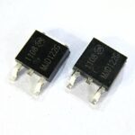
NE556ST SOIC
The NE556, SA556 and SE556 dual monolithic timing circuits are highly stable controllers capable of producing accurate time delays or oscillation. In the time delay mode of operation, the time is precisely controlled by one external resistor and capacitor. For a stable operation as an oscillator, the free running frequency and the duty cycle are both accurately controlled with two external resistors and one capacitor.
The circuits may be triggered and reset on falling waveforms, and the output structure can source or sink up to 200 mA.
All features
- TTL compatible
- Adjustable duty cycle
- Low turn-off time
- Timing from microseconds to hours
- Maximum operating frequency greater than 500 kHz
- Output can source or sink up to 200 mA
- Temperature stability of 0.005% per °C
- Operates in both astable and monostable modes
Related products
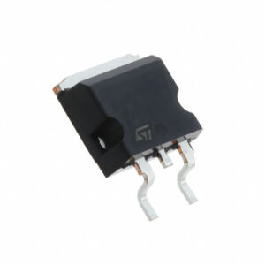
7812ST TO263
The L78 series of three-terminal positive regulators is available in TO-220, TO-220FP, D²PAK and DPAK packages and several fixed output voltages, making it useful in a wide range of applications.
These regulators can provide local on-card regulation, eliminating the distribution problems associated with single point regulation. Each type embeds internal current limiting, thermal shut-down and safe area protection, making it essentially indestructible. If adequate heat sinking is provided, they can deliver over 1 A output current. Although designed primarily as fixed voltage regulators, these devices can be used with external components to obtain adjustable voltage and currents.
7815 ST TO263
The L78 series of three-terminal positive regulators is available in TO-220, TO-220FP, D²PAK and DPAK packages and several fixed output voltages, making it useful in a wide range of applications.
These regulators can provide local on-card regulation, eliminating the distribution problems associated with single point regulation. Each type embeds internal current limiting, thermal shut-down and safe area protection, making it essentially indestructible. If adequate heat sinking is provided, they can deliver over 1 A output current. Although designed primarily as fixed voltage regulators, these devices can be used with external components to obtain adjustable voltage and currents.
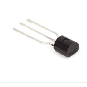
78L05ST SOT89
The L78L series of three-terminal positive regulators employ internal current limiting and thermal shutdown, making them essentially indestructible. If adequate heat-sink is provided, they can deliver up to 100 mA output current. They are intended as fixed voltage regulators in a wide range of applications including local or on-card regulation for elimination of noise and distribution problems associated with single-point regulation. In addition, they can be used with power pass elements to make high-current voltage regulators. The L78L series used as Zener diode/resistor combination replacement, offers e improvement along with lower quiescent current and lower noise.

CD4051ST SOIC
The HCF4051 device is a monolithic integrated circuit fabricated in MOS (metal oxide semiconductor) technology available in SO-16 and PDIP-16 packages.
The HCF4051 analog multiplexer/demultiplexer is a digitally controlled analog switch having low ON impedance and very low OFF leakage current. This multiplexer circuit dissipates extremely low quiescent power over the full VDD- VSSand VDD- VEEsupply voltage range, independent of the logic state of the control signals.
This device is a single 8-channel multiplexer having three binary control inputs, A, B, and C, and an inhibit input. The three binary signals select 1 of 8 channels to be turned on, and connect one of the 8 inputs to the output. When a logic “1” is present at the inhibit input terminal all channels are off.

L6561ST SOIC
L6561 is the improved version of the L6560 standard Power Factor Corrector. Fully compatible with the standard version, it has a superior performant multiplier making the device capable of working in wide input voltage range applications (from 85V to 265V) with an excellent THD. Furthermore the start up current has been reduced at few tens of mA and a disable function has been implemented on the ZCD pin, guaranteeing lower current consumption in stand by mode.
Realised in mixed BCD technology, the chip gives the following benefits: micro power start up current 1% precision internal reference voltage (T j = 25°C) Soft Output Over Voltage Protection no need for external low pass filter on the current sense very low operating quiescent current minimises power dissipation
The totem pole output stage is capable of driving a Power MOS or IGBT with source and sink currents of ±400mA. The device is operating in transition mode and it is optimised for Electronic Lamp Ballast application, AC-DC adaptors and SMPS.